Video Article Open Access
Advanced ZnO Based Piezo-Phototronic Optoelectronics
Wenbo Peng
School of Microelectronics, Xi’an Jiaotong University, Xi’an, 710049, China
Vid. Proc. Adv. Mater., Volume 3, Article ID 2210353 (2022)
DOI: 10.5185/vpoam.2022.10353
Publication Date (Web): 17 Oct 2023
Copyright © IAAM
Graphical Abstract
Abstract
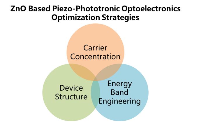
Since its invention in 2010, piezo-phototronic effect has been widely used in piezoelectric semiconductor materials and optoelectronic devices, e.g., solar cells, light-emitting diodes, and photodetectors, for both fundamentally physical research and potential applications. However, so far, the most related researches are mainly focused on whether piezo-phototronic effect could modulate the devices’ performance, and the reported piezo-phototronic effect induced enhancement is varying from a few dozen percent to thousands percent. Why the piezo-phototronic effect could induce such different performance improvements in different optoelectronic devices? In some special cases, the piezo-phototronic effect even causes performance degradation. Therefore, it is of great significance to carefully investigate the role of the piezo-phototronic effect plays in different optoelectronic devices, which might possibly give us more clear understandings of the piezo-phototronic effect and further constructive suggestions of how to utilize it more effectively. In our recent works in the past a few years, we have systematically studied the piezo-phototronic effect in optoelectronic devices using ZnO as the piezoelectric semiconductor material, including: photodiodes with different device structures [1], thin-film transistors with different charge carrier concentrations [2], and heterojunctions with different energy band diagram alignments [3], to reveal the underlying physics in piezo-phototronic effect. Our experimental and theoretical results indicate that: (1) the charge carrier concentration in ZnO is of great importance, should not being too small or too large; (2) compared to isotype photodiodes, anisotype photodiodes are preferred; (3) energy band diagram alignment is also preferred since misalignment would cause negative effects when introducing the piezo-phototronic effect. At last, we give a systematic instruction on how to utilize the piezo-phototronic effect more effectively.
Keywords
ZnO; piezo-phototronic; optoelectronic.
Acknowledgement
This research was supported by the National Natural Science Foundation of China (Grant No. 62174131 and 61704135), the China Postdoctoral Science Foundation (Grant No. 2018T111055 and 2017M613138), the Postdoctoral Research Project of Shaanxi Province (Grant No. 2017BSHEDZZ30).
References
- Z. Pan, W. Peng, F. Li, and Y. He, Advanced Functional Materials, 2018, 28, 1706897.
- Z. Pan, W. Peng, F. Li, and Y. He, Nano Energy, 2018, 49, 529-537.
- F. Li, W. Peng, Z. Pan, and Y. He, Nano Energy, 2018, 48, 27-34.
Video Proceedings of Advanced Materials

Upcoming Congress
