Video Article Open Access
Gallium Nitride Technology for Future Ultraviolet Light Emitting, Detecting and Electronic Devices
Haiding Sun
School of Microelectronics, University of Science and Technology of China, Hefei, Anhui 230026, China
Vid. Proc. Adv. Mater., Volume 2, Article ID 202110236 (2021)
DOI: 10.5185/vpoam.2021.10236
Publication Date (Web): 15 Apr 2022
Copyright © IAAM
Graphical Abstract
Abstract
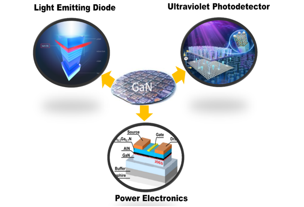
The III-nitride family (AlN, GaN, InN, and their alloys) has been regarded as one of the most significant semiconductors, and has therefore been heavily investigated in the past two decades for both optoelectronics (light emitting diodes, photodetectors, etc.), and power electronics applications (high mobility electron transistor, etc) [1]. Excitingly, the InGaN-based light emitters have revolutionized the lighting industry, promoting energy-efficient and eco-friendly modern solid-state lighting and lasing technologies. Similarly, by alloying GaN with AlN, we can synthesize AlGaN ternary alloys with tunable direct bandgaps from 3.4 eV (GaN) to 6.1 eV (AlN), corresponding to a wide UV spectral range from 360 nm to 210 nm, for a broad range of applications including air/water purification, UV curing, data storage, optical communication, etc. Hence, the AlGaN alloys have attracted enormous attention in the nitride community for use in efficient AlGaN-based UV LED [2,3], lasers and photodetectors [4]. In the field of power electronics, AlGaN alloys possess superb material properties including large critical electric fields, high electron mobility, and an excellent power figure of merit, making them very suitable for developing power electronic devices [5]. In this presentation, we will focus on the development of AlGaN-based high efficient UV LEDs, UV lasers, UV detectors as well as AlGaN/GaN heterojunction based HEMTs. Particularly, we will discuss the successful demonstration of the high efficient deep-ultraviolet light-emitting diodes grown on large misoriented sapphire substrates, ultraviolet lasers in the form of graded index separated confinement heterostructure (GRINSCH), the high photoresponsive solar-blind photodetectors in the form of AlGaN-based nanowires, as well as the high performance of HEMT. In the first part, high quality Al1-xGaxN/Al1-yGayN multiple quantum wells (MQWs) with sharp interfaces and emitting at ~280 nm was successfully grown on sapphire substrate with a misorientation angle as large as 4°. Wavy MQWs are observed due to step bunching formed at the step edges of the highly misoriented substrate. A significantly enhanced photoluminescence intensity (at least 10 times higher), improved internal quantum efficiency over 90%, and a much longer carrier lifetime were achieved for QWs grown on 4° misoriented sapphire substrate when compared with that grown on 0.2° misoriented sapphire. Importantly, the wafer-level output power of the ultraviolet light emitting diodes on 4° misoriented sapphire substrate were nearly doubled. In the second part, we will discuss about the UV lasers in the form of GRINSCH. In the third part, we will discuss the research on the solar-blind PDs based on self-assembled defect-free wide bandgap AlGaN nanowires on the low cost, large-scale silicon substrate, demonstrating superior photoresponse capability with high reproducibility, reliability and scalability. And in the last part, we will cover recent progress of development of high performance AlGaN/GaN based HEMT devices.
Keywords
Gallium nitride; light emitting diode; ultraviolet photodetector; power electronics, HEMT.
Acknowledgement
This work was funded by National Science Foundation of China (Grant No. 61905236), University of Science and Technology of China (Grant No. KY2100000081), the Fundamental Research Funds for the Central Universities (Grant No. WK2100230020).
References
- H. Zhang, C. Huang, K. Song, H. Yu, C. Xing, D. Wang, Z. Liu, and H. Sun, Reports on Progress Physics, 2021, 84(4), 044401.
- H. Sun, S. Mitra, R. C. Subedi, Y. Zhang, W. Guo, J. Ye, M. K. Shakfa, T. K. Ng, B. S. Ooi, I. S. Roqan, Z. Zhang, J. Dai, C. Chen, and S. Long, Advanced Functional Materials, 2019, 29 (48), 1905445.
- Yu, H., M. H. Memon, D. Wang, Z. Ren, H. Zhang, C. Huang, M. Tian, H. Sun*, and S. Long. Optics Letters, 2021, 46(13), 3271-3274.
- D. Wang, X. Liu, S. Fang, C. Huang, Y. Kang, H. Yu, Z. Liu, H. Zhang, R. Long, Y. Xiong, Y. Lin, Y. Yue, B. Ge, T. Ng, B. S. Ooi, Z. Mi, J. He, and H. Sun, Nano Letters, 2021, 21(1), 120.
- H. Zhang, Liang, F., Song, K., Xing, C., Wang, D., Yu, H., Huang, C., Sun, Y., Yang, L., Zhao, X. and H Sun*, Long, S., Applied Physics Letters, 2021, 118(24), 242105.
Biography
Haiding Sun received his Ph.D. in Electrical Engineering from Boston University. He is a Professor in the School of Microelectronics at University of Science and Technology of China. He has published 90+ peer-reviewed SCI-index journal papers including Nature Electronics, Advanced Functional Materials, Nano Letters, IEEE Electron Device Letters, Applied Physics Letters, Optics Letters and Optics Express etc. He has written 4 book chapters and holds 4 US, 4 PTC and 30 Chinese Patents. His research interests include the investigation of the physics, MBE and MOCVD epitaxy, fabrication, and characterization of wide bandgap semiconductor materials for both optoelectronics and electronic devices. This includes nanostructures and low-dimensional structures (quantum wires, dots, wells) for nanoelectronics and nanophotonics, based on group III-Nitrides and III-Oxides. His work has been highlighted by more than 100 times in many media outlets including Compound Semiconductors, Semiconductors Today, Phys.org, Nanowerk etc. He is currently Associated Editor of 《IEEE Photonics Technology Letters》, 《SPIE Journal of Nanophotonics》, 《ASME Open Journal of Engineering》, and Guest Editor of《Journal of Electronic Packaging》and 《Crystal》. He is a IEEE Senior Member, and the recipient of the 2021 iCANX Young Scientist Award and 2021 IAAM Young Scientist Medal.
Video Proceedings of Advanced Materials
Upcoming Congress
