Video Article Open Access
Boron Nitride Nanotube/nanosheet for Energy and Environmental Applications
Yoshio Bando1,2,3
1Australian Institute for Innovative Materials, University of Wollongong, Squires Way, North Wollongong, NSW 2500, Australia
2Institute of Molecular Plus, Tianjin University. No. 11 Building, No. 92 Weijin Road, Nankai District, Tianjin, 300072, P. R. China
3International Center for Materials Nanoarchitectonics (WPI-MANA), National Institute for Materials Science, 1-1 Namiki, Tsukuba, Ibaraki, 305-0044, Japan
Vid. Proc. Adv. Mater., Volume 1, Article ID 2020-0837 (2020)
DOI: 10.5185/vpoam.2020.0837
Publication Date (Web): 10 Nov 2020
Copyright © IAAM
Graphical Abstract
Abstract
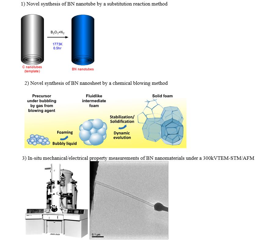
The highly efficient thermal management is particularly important for quick heat release in the face of increasing power consumption of electronic devices. Moreover, high-energy high-power electricity storage is key to next-generation electronic and electric devices. Hexagonal boron nitride (h-BN), a layered material with a regular network of BN hexagons, is a structural sister system of famous graphite. BN is highly insulating and wide bandgap in properties, and more stable than graphite in thermology and chemistry. These make BN be a perfect sidekick of graphite nanomaterials, and enable their bright prospects in high thermal conductivity, strong ultraviolet emission, glorious thermal and chemical inertness, rubout insulation and superb lubrication. However, their insufficient production rather limited the studies and the full realization of potentials. We aim to develop new nanomaterials such as nanotubes and nanosheets in boron-carbon-nitrogen system for their applications to thermal conductive packaging as well as energy storage. We have recently developed effective methods for the high-yield syntheses of BN nanotubes and nanosheets. We have synthesized gram-level high-quality BN nanotubes through the carbon free- chemical vapor deposition and gram-level nanosheets by the chemical blowing method, which make them possible to initiate the studies of polymetric composites. Thin BN nanotubes with diameter less than 10 nm were fabricated successfully by optimizing the reaction of metal oxide and boron source. BN nanosheets with average around 5 nm were effectively realized via polymerization and crystallization of ammonia borane, based on the chemical blowing method. Our BN nanotubes and nanosheets have been filled into polymer matrix to make thermal conductive composites, which were created with 20-times increase of original thermal conductivity. They are useful for heating-release insulting packaging of down-sizing faster cooler electronics. Due to the special polarity of boron nitrogen bonding, the BN nanomaterials with high specific surface area have also been developed and applied to dense hydrogen uptake. Our synthesis methods are thus extended for producing new graphene materials, e.g. 3D strutted graphene (SG) via chemical blowing. The SG consists of continuous graphitic membranes which are homogenously connected and spatially supported by the networks of micrometre-width graphitic struts. The high electrical conductivity, specific surface area, mechanical strength and elasticity are thus simultaneously achieved. In addition, we indeed demonstrate the striking effects of tensile, compressive, and bending deformation on the electrical response of BN nanotubes and nanosheets under manipulation and electrical probing in a 300kV HRTEM using STM/AFM-TEM special holders. The bending forces of BN nanotubes are directly measured inside HRTEM and real-time video-recording of elastic kinking deformation (that reveals a superb BN nanotube flexibility) is performed. We conclude here that BN nanotubes have a high potential for the applications in novel nanoscale sensors, actuators, and advanced nanoelectromechanical systems (NEMS).
Keywords
Boron nitride, nanotube, nanosheet, novel synthesis, energy application, in-situ TEM.
Acknowledgement
I would like to acknowledge my collaborators, Drs. D. Golberg, C. Tang, C. Zhi, W. Han, D. Tang and others in NIMS, Japan.
References
- D. Golberg, Y. Bando, Y. Huang, T. Terao, M. Mitome, C. Tang, C. Zhi, ACS nano, 2010, 4(6), 2979.
- C. Zhi, Y. Bando, C. Tang, H. Kuwahara, D. Golberg, Advanced Materials, 2009, 21, 2889.
- W. Han, Y. Bando, K. Kurashima, T. Sato, Applied Physics Letters, 1998, 73, 3085.
- X. Wang, Y. Zhang, C. Zhi, X. Wang, D. Tang, Y. Xu, Q. Weng, X. Jiang, Y. Bando, Nature Communications, 2013, 4, 1.
- D. Tang, X. Wei, Y. Bando, Y., D. Golberg, Nano Lett., 2012, 12, 1898.
Biography
Yoshio Bando has been leading the communities of nanomaterials and electron microscopy for many years. Holding a PhD degree from Osaka University, he joined the National Institute for Research in Inorganic Materials (NIRIM) in 1975. In 2001, NIRIM was merged with the National Research Institute for Metals to form the National Institute for Materials Science (NIMS), and he was appointed as Director of the Advanced Beam Analysis Group, followed by being appointed Director-General of International Center for Young Scientist. He became a NIMS Fellow in 2004. From 2008 to March 2017, he was responsible for the operation of MANA with the appointed position of Chief Operating Officer (COO). In addition, he was adjunct professor of University of Tokyo (2009-2012) and guest professor of Waseda University (2008-2016). After retirement of NIMS in 2017, he has been appointed as Distinguished Professor at the University of Wollongong, Australia, and honorary Fellow of NIMS. He is now also Professor at Institute for Molecular Plus, Tianjin University China. He has received many prestigious awards and fellowships, including the "Sacred Treasure" given from the Japanese Emperor in 2017, The 3rd Thomson Reuters Research Front Award in 2012, The Tsukuba Prize in 2005, Academician, The Commendation Award by the Minister of State for Science and Technology in 1998, The Academic Award of the Ceramic Society of Japan in 1997, The Seto Award of Electron Microscopy Society of Japan in 1994 and others. He was appointed as adjunct member of the Science Council of Japan in 2006. He is also a Fellow of the American Ceramic Society and the Royal Society of Chemistry. He served as Editor-in-Chief of Journal of Electron Microscopy and Editorial Board Members of "Nano Energy", "Small", "Nanotechnology", "Materials Horizon", “Nanomaterials” and others. He has been selected as ISI Highly Cited Researcher in Materials Science in 2010, 2012, 2014, 2015, 2016 2017, 2018 and 2019. To date, he has authored 840 original research papers that have been cited more than 50,341 times with h-index of 117 (Web of Science in January 2020). He has been registered 43 foreign patents and 70 Japanese patents.
Video Proceedings of Advanced Materials
Upcoming Congress
